

Post-CMOS packaging methods for integrated biosensors
Abstract
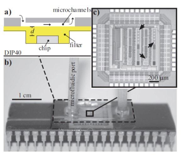
We report on several techniques that have been pursued in our laboratories for packaging complementary metal-oxide semiconductor (CMOS) sensors for use in biological environments, such as cell medium. These techniques are suited for single CMOS die ranging from 1.5 × 1.5 mm2 to 3 × 3 mm2 in area. The first method consisted of creating high aspect ratio structures from negative-tone photocurable resins to simultaneously encapsulate wirebonds from the chip to a ceramic package and create a cell culture well. The second technique used a photolithographically defined barrier on the die to allow the use of non-photocurable resins as encapsulants. The third method consisted of re-routing the die padframe using photolithographically defined, planar leads to a much larger padframe; this will allow the chip to be integrated with microfluidic networks. Finally, we show a method in which the encapsulant was also used as an optical filter and as a base for integrating more complex structures.
